
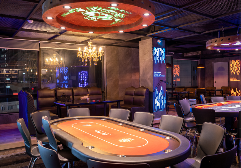
카지노사이트: 안전한 온라인 도박의 선택
카지노사이트를 찾고 계신가요? 안전하고 신뢰할 수 있는 온라인 도박 사이트를 찾는 것은 매우 중요합니다. 현대 사회에서는 다양한 온라인 카지노 사이트가 존재하지만, 그 중에서도 안전성과 신뢰성이 가장 중요한 요소입니다. 안전한 카지노사이트의 특징 카지노사이트를 선택할 때 주의해야 할 몇 가지 중요한 요소가 있습니다. 첫 번째로는 라이센스를 확인해야 합니다. 해당 사이트가 정품 라이센스를...
카지노사이트를 찾고 계신가요? 안전하고 신뢰할 수 있는 온라인 도박 사이트를 찾는 것은 매우 중요합니다. 현대 사회에서는 다양한 온라인 카지노 사이트가 존재하지만, 그 중에서도 안전성과 신뢰성이 가장 중요한 요소입니다. 안전한 카지노사이트의 특징 카지노사이트를 선택할 때 주의해야 할 몇 가지 중요한 요소가 있습니다. 첫 번째로는 라이센스를 확인해야 합니다. 해당 사이트가 정품 라이센스를...

온라인바라카는 온라인 카지노 게임 중 한 가지로, 최근 많은 이용자들에게 인기를 끌고 있습니다. 이 게임은 신뢰할 수 있는 보증과 함께 다양한 쿠폰, 이벤트, 그리고 프로모션을 제공하여 플레이어들에게 더욱 특별한 경험을 선사합니다. 온라인바라카를 즐기는 이용자들은 다양한 혜택을 누릴 수 있습니다. 예를 들어, 쿠폰을 활용하면 보다 저렴한 가격에 게임을 즐길 수 있습니다....

슬롯사이트에서 게임을 즐기는 것은 단순한 도박이 아닌 전략과 지식이 필요한 미니 게임입니다. 슬롯머신은 운이 좋을 때 큰 상금을 슬롯사이트 받을 수 있는 기회를 제공하지만, 보다 많은 이득을 얻기 위해서는 쿠폰, 이벤트 및 프로모션을 적극적으로 활용해야 합니다. 쿠폰은 슬롯사이트에서 무료로 제공되는 혜택으로, 보너스 포인트나 현금으로 환급받을 수 있습니다. 쿠폰을 활용하면 게임을...

바카라사이트는 현재 온라인 카지노 게임 중에서 가장 인기 있는 게임 중 하나입니다. 이 게임은 전략과 운을 모두 필요로 하며, 플레이어들에게 스릴과 재미를 제공합니다. 왜 바카라사이트를 선택해야 하는가? 바카라사이트는 간단한 규칙으로 인해 많은 사람들이 즐기는 게임입니다. 또한 고스톱과 비슷한 점이 있어 한국인들 사이에서도 인기가 많습니다. 또한 온라인 카지노에서 바카라를 즐길 수...
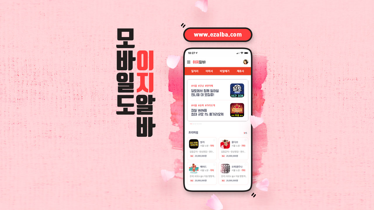
룸알바 소개 룸알바는 다양한 일자리를 제공하는 독보적인 플랫폼입니다. 이곳에서는 고수익의 알바를 쉽게 찾을 수 있으며, 사용자의 필요와 기술에 따라 맞춤형 일자리를 추천받을 수 있습니다. 이지알바 커뮤니티는 사용자들에게 실시간 업데이트되는 다양한 일자리 정보를 제공하며, 지역별, 업종별로 상세한 업체 정보를 소개합니다. 이곳에서는 누구나 자신에게 맞는 일자리를 찾고, 안정적인 수입을 얻을 수 있습니다....
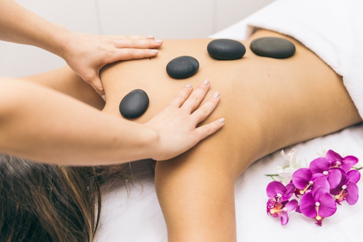
마사지 커뮤니티의 정의와 스웨디시쏘의 역할 마사지 커뮤니티는 사람들이 마사지에 대한 경험, 정보, 그리고 리뷰를 공유하는 공간입니다. 이런 커뮤니티에서 스웨디시쏘의 역할은 중요합니다. 스웨디시쏘는 사용자들에게 신뢰할 수 있는 마사지 업체 정보를 제공하며, 가격 비교, 업체 리뷰, 그리고 이용 후기를 통해 최적의 마사지 경험을 찾도록 돕습니다. 이는 마사지 문화를 더욱 풍부하고 접근하기 쉬운...

안전놀이터 소개 안전놀이터는 사용자들에게 검증된 엔터테인먼트 경험을 제공하는 플랫폼입니다. 이곳에서는 이용자의 안전과 즐거움이 최우선입니다. 이박사는 안전놀이터를 추천하고, 사용자들에게 신뢰할 수 있는 정보를 제공하며, 이들을 위한 가장 안전한 업체들을 선별하여 소개합니다. 이곳의 모든 업체는 엄격한 기준을 통해 검증되어 사용자들이 안심하고 즐길 수 있는 환경을 제공합니다. 자세한 정보는 공식 홈페이지에서 확인할 수...

파워볼 통계 분석: 데이터가 말하는 승리의 비밀 파워볼 게임은 숫자의 마법과 확률의 놀라운 세계에서 시작됩니다. 베픽 커뮤니티에서 제공하는 파워볼 통계 분석은 이러한 게임의 복잡성을 단순화하며, 사용자들에게 데이터 기반의 명확한 통찰력을 제공합니다. 우리의 분석기는 과거 데이터, 승률, 빈도수 등을 종합적으로 분석하여, 각 숫자의 가능성을 예측합니다. 이러한 방식은 파워볼 게임에 접근하는 새로운...

우리카지노 소개 우리카지노는 온라인 게임과 카지노의 세계에서 빛나는 별입니다. 이 플랫폼은 사용자에게 다양한 게임 옵션과 함께 끊임없는 재미를 제공합니다. 카지노친구, 우리카지노의 파트너,는 신뢰할 수 있는 추천과 보증을 통해 사용자들에게 최상의 게임 경험을 보장합니다. 여기서는 빅데이터 기반의 철저한 검증을 거친 업체들만을 소개하므로, 안전하고 신뢰할 수 있는 게임 환경을 제공합니다. 인기 있는...

런던토토 소개 런던토토는 온라인 카지노 시장에서 두각을 나타내는 플랫폼으로, 사용자들에게 최상의 카지노 경험을 제공하기 위해 끊임없이 노력합니다. 런던토토는 사용자 친화적인 인터페이스, 다양한 게임 옵션, 그리고 안전한 환경을 제공함으로써 게임을 더욱 즐겁고 편리하게 만듭니다. 이 플랫폼은 게임의 공정성과 사용자의 안전을 최우선으로 여기며, 이를 위해 철저한 보안 조치를 취하고 있습니다. 또한, 사용자들이...

안전놀이터: 신뢰와 보안의 기준 안전놀이터의 중요성은 이제 누구나 인정하는 사실입니다. 토토친구는 사용자의 안전을 최우선으로 여기며, 엄선된 보증업체들을 통해 믿을 수 있는 게임 환경을 제공합니다. 이 플랫폼은 사용자들에게 안전한 베팅 환경을 제공하며, 신뢰할 수 있는 업체들만을 소개하여 사용자들이 안심하고 즐길 수 있도록 합니다. 토토친구: 사용자 중심의 플랫폼 토토친구는 사용자의 편의를 생각하는...

베픽 커뮤니티 소개 베픽 커뮤니티는 사용자들에게 파워볼 통계 분석을 제공하는 공간입니다. 여기서는 대규모 데이터를 기반으로 한 분석이 진행되며, 이는 사용자들이 더 정확하고 신뢰할 수 있는 정보를 얻을 수 있게 합니다. 이 커뮤니티는 최신 트렌드를 반영하며, 사용자들이 파워볼 게임에서 더 나은 결정을 내릴 수 있도록 돕습니다. 베픽의 목표는 사용자들에게 질 높은...

스웨디시 마사지는 근육의 긴장을 풀고 전반적인 이완을 촉진하는 스웨덴에서 유래된 마사지 기법입니다. 이 마사지는 일반적으로 오일을 사용하며, 부드러운 긴 스트로크와 함께 근육을 쓸어내리고 주무르는 동작이 포함됩니다. 스웨디시 마사지의 효과는 개인마다 다를 수 있지만, 대체로 스트레스 감소, 혈액 순환 개선, 그리고 긴장된 근육의 이완에 도움을 준다고 알려져 있습니다. 이러한 효과는 일상의...
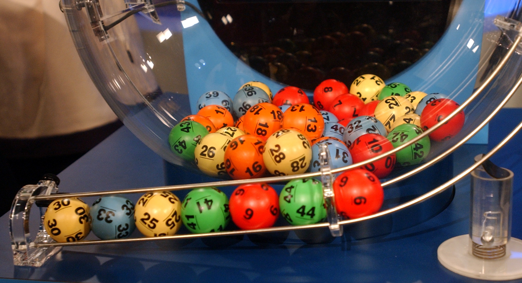
로또 번호 선택에 고민이라면, 프리또에서 제공하는 무료 로또번호 생성 서비스를 경험해보세요. AI 기반 기술로 분석한 확률과 통계를 바탕으로, 매주 당첨 가능성이 높은 번호들을 제안합니다. 로또 645의 당첨 번호를 예측하는 것은 언제나 흥미롭습니다. 복잡한 빅데이터 분석과 인공지능의 예측 알고리즘을 통해, 우리는 더 이상 무작위 선택에 의존하지 않습니다. 이번 주의 추천 번호는...

라칸카지노에 오신 것을 환영합니다! 이곳에서는 가장 흥미진진한 카지노 경험을 기대하실 수 있습니다. 첫 방문이신가요? 걱정하지 마세요! 이 글을 통해 라칸카지노의 모든 것을 알려드릴게요. 간단한 가입 방법부터 다양한 프로모션까지, 이제 카지노의 세계에 발을 들이실 준비가 됐습니다. 1. 가입 방법 라칸카지노의 가입은 간단합니다. 홈페이지에 접속한 후, ‘회원가입’ 버튼을 클릭하고 요구되는 정보를 입력하면...